Overview
System Overview
The goal of this project was to design an analog style synthesizer with an instrument that makes sound when you spin it, press keys or turn knobs, using a microcontroller (MCU) and field-programmable gate array (FPGA). The project would generate real time audio controlled by a digital gyroscope, keypad, and knobs.
The gyroscope is be mounted on a spinning device, and its rotational velocity is read by the MCU. Simultaneously, 8 keys are connected to the MCU’s digital GPIO pins to choose from 8 distinct frequencies for an audio signal. Additionally, the MCU will use its built-in ADC peripheral to convert a voltage in an analog pin (controlled externally with the potentiometer knob) to a 4-bit digital value.
The original plan was to have two independent audio outputs, each corresponding to a distinct input source. One frequency would be calculated based on the angular velocity of the gyroscope, and the other frequency would depend on which of the 8 keys in the keypad were pressed. We unfortunately did not reach the point of driving a speaker based on the gyroscope’s input, but we were able to control one speaker based on the keypad.
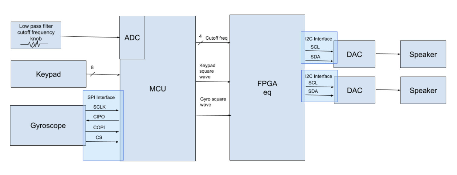
The original plan was for the MCU to handle all user input (from the gyroscope, keypad, and potentiometer knob), and to forward those results (two square waves, and 4 bits encoding the potentiometer knob reading) to the FPGA for processing. The FPGA would then filter the digital waveforms using a FIR low-pass filter, with the cutoff frequency determined by the potentiometer reading. Then, the FPGA would send the filtered audio signals to two DACs over I2C to ultimately drive two speakers. Due to unforeseen challenges, we ended up not filtering the audio signal and driving the speakers directly with the MCU.
In the end, we created a digital audio synthesizer with 8 distinct inputs based on a keypad. The device also is also able to read the rotational velocity of a gyroscope along 3 axes, as well as analog voltage input to the MCU. Beyond that, we designed (but did not complete the implementation of) an FIR low-pass filter and I2C communication on the FPGA.
The aspects of this project that make it unique compared to E155 labs include usage of the MCU’s ADC peripheral and the FPGA’s I2C and sysDSP peripherals.
Block Diagram
Below is a block diagram representing the entire (planned) project:
Unfortunately, due to unforeseen challenges (both within and outside the scope of the project), we did not get to complete the FPGA design of the project. Below is a block diagram representing how the project actually turned out:
