FPGA Design
FPGA Design Plan
This project uses the iCE40 UP5K FPGA on the UPdino v3.1 development board. Originally, the FPGA was intended to act as a hardware accelerator for audio equalization. Specifically, the FPGA would apply a low-pass finite impule response (FIR) filter to a square wave generated by the MCU. The MCU would send two square waves to the FPGA–one of the frequency corresponding to the pressed key, and one of the frequency corresponding to the gyroscope’s angular speed– connected by wire.
In addition, the MCU would send the desired cutoff frequency of the low-pass filter, encoded with 4 bits, and also transmitted over wires. However, SPI also could have been used to transmit the cutoff frequency in order to increase resolution. The 4-bit cutoff frequency value would correspond to frequency spanning from 200 to 1600 Hz. This range was designed with the intended keypad range of middle C (~261 Hz) to C5 (~523 Hz), so 200-1600Hz should be an effective range of cutoff frequencies for the low-pass filter.
Internally, a divided clock based on the HSOSC IP module would be used to generate a 44kHz signal to sample the audio inputs. This frequency was selected because 44kHz is double the highest audible audio frequency, making it a standard audio sampling frequency. The audio data would be sampled into a 51-bit wide shift register. Simultaneously, 51 16-bit taps corresponding to the cutoff frequency would be read in from BRAM. These taps would be convolved with the shift register of past inputs in order to calculate the current audio output. This would be accomplished using the sysDSP IP block SB_MAC16 (multiply and accumulate) primitive on the iCE40.
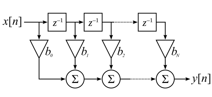
Since the input is a square wave, the multiplication of each previous input with the corresponding tap should be relatively straightforward. The main source of complexity would be in the accumulation of all 51 taps. Executing all of this combinational logic would be challenge to fit within one clock cycle, giving rise to timing issues. As a result, this process would have to be pipelined, running over multiple clock cycles. Assuming the FPGA clock (based on HSOSC) is running at 40MHz and the FPGA is sampling the input at 44kHz, 900 processing cycles could fit within the time between samples. 900 cycles is more than enough to accumulate 51 16-bit precision taps. Thus, timing is not a concern with pipelining the FIR filter.
In order to hold the FIR filter output steady while the FIR filter is generating the next output, a synchronous enabled flop would be used to control the input to and output from the FIR filter module. This flop would be enabled based on an input ready signal, based on the 44kHz sampling signal, and output ready signal, driven by the controller of the FIR filter datapath.
There would be two instances of the FIR filter module, one for the MCU output driven by the keypad, and the other for the MCU output driven by the gyroscope. The outputs of the FIR filters then would be converted to 8-bit audio values, which would then be transmitted over The DACs would then be used to drive two speakers. I2C would be implemented using the built-in I2C IP on the iCE40. The iCE40 can support up to 2 sets of I2C busses. The MCP4725 DAC supports a standard 100 kHz communication frequency, as well as a 400 kHz fast mode and a 3.4 MHz high-speed mode. Additionally, the DAC must be sent 4 bytes (or 32 bits) in every transaction writing to the DAC Input Register. This means that the DAC fast mode speed of 400 kHz would be more than sufficient to drive audio at 44kHz.
Filter Design
The FIR low-pass filter was designed to have 51 taps using the window method, as implemented by the firwin function in the SciPy Signal Processing library. This number was determined experimentally. Through trials with a varying number of taps, 51 was one of the lowest numbers where the audio filtering was noticeable. The 51 taps were then calculated for 15 cutoff frequencies, spanning from 200 Hz to 1.6 kHz.
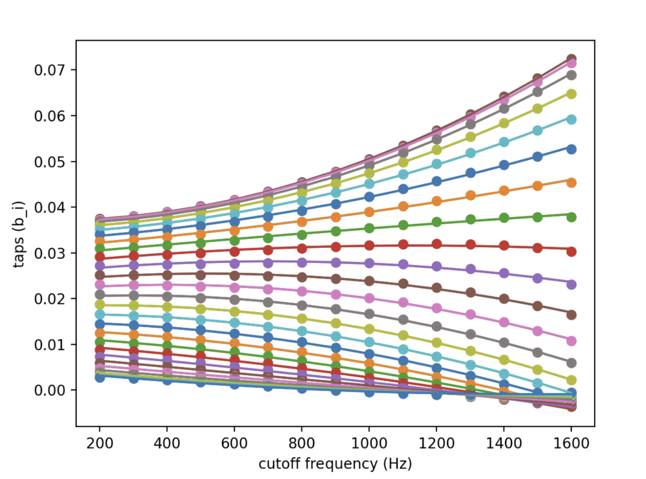
All of these taps were then converted to 16-bit 2s-complement, and loaded into BRAM. An itial idea was to calculate the 51 taps using lines of best fit (selected by cutoff frequency), but the necessary precision would have required floating-point arithmetic, which is not supported on the FPGA.
FPGA Design Reality
Due to unforeseen circumstances, we had to rescope the project to greatly simplify the role of the FPGA in this project. Initially, the FIR filter was removed from the project entirely, leaving the FPGA to serve as a buffer between the MCU’s square wave outputs and the DACs. The data that previously encoded the FIR filter cutoff frequency would instead be used to control output volume. So, the FPGA would read in the two square waves from the MCU at 44kHz, scale them by an amount proportional to the 4-bit volume value, and send this result over I2C to the two DACs to ultimately drive the two speakers with two square waves at the specified volume.
Unfortunately, the microcontroller and hardware design aspects of the project took longer than expected, and we did not complete the rescoped FPGA design.
References
DSP for FPGA: Simple FIR Filter in Verilog - Whitney Knitter, Hackster.io